(Hong Kong)

Product Summary
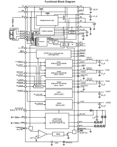
The TPS65070RSLR is a single chip Power Managemen IC for portable applications consisting of a batter charger with power path management for a single Li-Ion or Li-Polymer cell. The charger can either be supplied by a USB port on pin USB or by a dc voltage from a wall adapter connected to pin AC . Three highly efficient 2.25MHz step-down converters are targeted at providing the core voltage, memory and I/O voltage in a processor based system. The TPS65070RSLR enters a low power mode at ligh load for maximum efficiency across the wides possible range of load currents. For low noise applications the TPS65070RSLR can be forced into fixed frequency PWM using the I2C interface. The applications of the TPS65070RSLR include Portable Navigation Systems, PDAs, Pocket PCs, OMAP and Low Power DSP Supply.
Parametrics
TPS65070RSLR absolute maximum ratings: (1)Voltage range on all pins except the pins listed below with respect to AGND: –0.3 to 7V; (2)Voltage range on pins INT , RESET , PGOOD, PB_OUT with respect to AGND: – 0.3 to V(AVDD6); (3)Voltage range on pins VINDCDC1/2, VINDCDC3, VINLDO respect to AGND: – 0.3 to V(SYS); (4)Voltage range on pins AD_IN1, AD_IN2, AD_IN3, AD_IN4 with respect to AGND : – 0.3 to 3.3 V; (5)Voltage range on pins ISINK1, ISINK2, AC, USB: – 0.3 to 20 V; (6)Voltage range on pin L4 (output voltage of boost converter), FB_wLED: – 0.3 to 40 V; (7)Current at SYS, AC, USB, BAT, L3: 3000 mA; (8)Current at all other pins: 1000 mA; (9)Continuous total power dissipation See Dissipation Rating Table; (10)Operating free-air temperature, T A: 40 to 85℃; (11)Maximum junction temperature, T J: 125℃; (12)Storage temperature, T st: –65 to 150℃; (13)Lead temperature 1,6 mm (1/16-inch) from case for 10 seconds: 260℃.
Features
TPS65070RSLR features: (1)2A Output Current on the Power Path; (2)Linear Charger; 1.5A Maximum Charge Current; (3)100mA/500mA/ 800mA/1300mA Curren Limit From USB Input; (4)Thermal Regulation, Safety Timers; (5)Temperature Sense Input; (6)2.25MHz Fixed Frequency Operation; (7)Up to 1.5A of Output Current; (8)Adjustable or Fixed Output Voltage; (9)V IN Range From 2.8V to 6.3V; (10)Power Save Mode at Light Load Current; (11)Output Voltage Accuracy in PWM Mode ± 1.5%; (12)Typical 19 μ A Quiescent per Converter.
Diagrams
| Image | Part No | Mfg | Description |  |
Pricing (USD) |
Quantity | ||||||||||||
|---|---|---|---|---|---|---|---|---|---|---|---|---|---|---|---|---|---|---|
 |
 TPS65070RSLR |
Texas Instruments |
PMIC Solutions 5Ch Pwr Mgmt IC |
Data Sheet |
|
|
||||||||||||
| Image | Part No | Mfg | Description | |
Pricing (USD) |
Quantity | ||||||||||||
 |
TPS60100 |
Other |
|
Data Sheet |
Negotiable |
|
||||||||||||
|
TPS60100EVM-131 |
Texas Instruments |
Power Management IC Development Tools 2 batt cells |
Data Sheet |
|
|
||||||||||||
|
TPS60100PWP |
Texas Instruments |
Charge Pumps Reg 3.3V Lo-Ns Chrg Pump DC-DC Cnvtr |
Data Sheet |
|
|
||||||||||||
|
TPS60100PWPG4 |
Texas Instruments |
Charge Pumps Reg 3.3V Lo-Ns Chrg Pump DC-DC Cnvtr |
Data Sheet |
|
|
||||||||||||
|
TPS60100PWPR |
Texas Instruments |
Charge Pumps Reg 3.3V Lo-Ns Chrg Pump DC-DC Cnvtr |
Data Sheet |
|
|
||||||||||||
|
TPS60100PWPRG4 |
Texas Instruments |
Charge Pumps Reg 3.3V Lo-Ns Chrg Pump DC-DC Cnvtr |
Data Sheet |
|
|
||||||||||||